练习九.利用状态机的嵌套实现层次结构化设计
目的:1.运用主状态机与子状态机产生层次化的逻辑设计;
2.在结构化设计中灵活使用任务(task)结构。
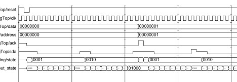
在上一节,我们学习了如何使用状态机的实例。实际上,单个有限状态机控制整个逻辑电路的运转在实际设计中是不多见,往往是状态机套用状态机,从而形成树状的控制核心。这一点也与我们提倡的层次化、结构化的自顶而下的设计方法相符,下面我们就将提供一个这样的示例以供大家学习。
该例是一个简化的EPROM的串行写入器。事实上,它是一个EPROM读写器设计中实现写功能的部分经删节得到的,去除了EPROM的启动、结束和EPROM控制字的写入等功能,只具备这样一个雏形。工作的步骤是:1.地址的串行写入;2.数据的串行写入;3.给信号源应答,信号源给出下一个操作对象;4.结束写操作。通过移位令并行数据得以一位一位输出。
模块源代码:
module writing(reset,clk,address,data,sda,ack);
input reset,clk;
input[7:0] data,address;
output sda,ack; //sda负责串行数据输出;
//ack是一个对象操作完毕后,模块给出的应答信号。
reg link_write; //link_write 决定何时输出。
reg[3:0] state; //主状态机的状态字。
reg[4:0] sh8out_state; //从状态机的状态字。
reg[7:0] sh8out_buf;//输入数据缓冲。
reg finish_F;//用以判断是否处理完一个操作对象。
reg ack;
parameter
idle=0,addr_write=1,data_write=2,stop_ack=3;
parameter
bit0=1,bit1=2,bit2=3,bit3=4,bit4=5,bit5=6,bit6=7,bit7=8;
assignsda = link_write? sh8out_buf[7] : 1'bz;
always @(posedge clk)
begin
if(!reset)//复位。
begin
link_write<= 0;
state<= idle;
finish_F <= 0;
sh8out_state<=idle;
ack<= 0;
sh8out_buf<=0;
end
else
case(state)
idle:
begin
link_write<= 0;
state<= idle;
finish_F <= 0;
sh8out_state<=idle;
ack<= 0;
sh8out_buf<=address;
state<= addr_write;
end
addr_write://地址的输入。
begin
if(finish_F==0)
beginshift8_out; end
else
begin
sh8out_state <= idle;
sh8out_buf<= data;
state <= data_write;
finish_F <= 0;
end
end
data_write://数据的写入。
begin
if(finish_F==0)
beginshift8_out; end
else
begin
link_write <= 0;
state <= stop_ack;
finish_F <= 0;
ack <= 1;
end
end
stop_ack://完成应答。
begin
ack <= 0;
state <= idle;
end
endcase
end
task shift8_out;//串行写入。
begin
case(sh8out_state)
idle:
begin
link_write<= 1;
sh8out_state <= bit0;
end
bit0:
begin
link_write <= 1;
sh8out_state <= bit1;
sh8out_buf <= sh8out_buf<<1;
end
bit1:
begin
sh8out_state<=bit2;
sh8out_buf<=sh8out_buf<<1;
end
bit2:
begin
sh8out_state<=bit3;
sh8out_buf<=sh8out_buf<<1;
end
bit3:
begin
sh8out_state<=bit4;
sh8out_buf<=sh8out_buf<<1;
end
bit4:
begin
sh8out_state<=bit5;
sh8out_buf<=sh8out_buf<<1;
end
bit5:
begin
sh8out_state<=bit6;
sh8out_buf<=sh8out_buf<<1;
end
bit6:
begin
sh8out_state<=bit7;
sh8out_buf<=sh8out_buf<<1;
end
bit7:
begin
link_write<= 0;
finish_F<=finish_F+1;
end
endcase
end
endtask
endmodule
测试模块源代码:
`timescale 1ns/100ps
`define clk_cycle 50
module writingTop;
reg reset,clk;
reg[7:0] data,address;
wire ack,sda;
always #`clk_cycleclk = ~clk;
initial
begin
clk=0;
reset=1;
data=0;
address=0;
#(2*`clk_cycle) reset=0;
#(2*`clk_cycle) reset=1;
#(100*`clk_cycle) $stop;
end
always @(posedge ack)//接收到应答信号后,给出下一个处理对象。
begin
data=data+1;
address=address+1;
end
writing writing(.reset(reset),.clk(clk),.data(data),
.address(address),.ack(ack),.sda(sda));
endmodule
仿真波形:
练习:仿照上例,编写一个实现EPROM内数据串行读取的模块。编写测试模块,给出仿真波形。
-
 热敏电阻温度阻值查询程序2024年11月13日 74
 -
C99语法规则2024年11月16日 675
-
 FreeRTOS 动态内存管理2024年11月12日 448
 -
一款常用buffer程序2024年11月06日 88
-
 1602液晶显示模块的应用2012年08月03日 192
 -
GNU C 9条扩展语法2024年11月18日 261
-
 如何实现STM32F407单片机的ADC转换2024年11月15日 300
 -
 STM32使用中断屏蔽寄存器BASEPRI保护临界段2024年11月15日 195
-
C99语法规则2024年11月16日 675
-
 51单片机LED16*16点阵滚动显示2012年09月05日 664
 -
FreeRTOS 动态内存管理2024年11月12日 448
-
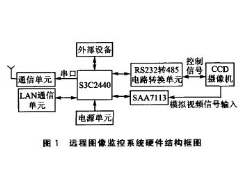 ARM9远程图像无线监控系统2012年07月03日 424
 -
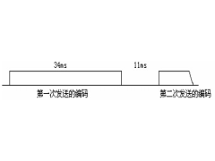 用单片机模拟2272软件解码2012年09月06日 300
 -
如何实现STM32F407单片机的ADC转换2024年11月15日 300
-
 新颖的单片机LED钟2012年08月06日 278
 -
GNU C 9条扩展语法2024年11月18日 261